


A broader overview of materials chemistry and structure using CISA
A comprehensive sample analysis often requires multiple instruments. Scanning electron microscopy (SEM) imaging and energy dispersive X-ray spectroscopy (EDX) can provide a wealth of surface topography and elemental composition information. However, this method may miss critical information about surface chemistry. Conversely, X-ray photoelectron spectroscopy (XPS) is a surface sensitive analysis technique, which reveals the surface chemistry of the materials, yet high-resolution imaging may still be necessary to clarify the chemistry-structure correlation and its impact on material properties. Here, Dr. Yahya Zakaria at Thermo Fisher Scientific explains why a correlative imaging and surface analysis (CISA) workflow enables a precise, broader analysis view.
The surface of a material is the main area that interacts with the environment in which it is situated, and so understanding a material’s surface chemistry is a key to unlocking its potential. A single method of analysis rarely paints the full picture, so materials scientists and engineers may need different characterisation methods to gain the right insights. Without combining techniques, essential findings can be missed, leading to unexpected changes in properties, performance issues or material failures. This is where a CISA workflow comes in.
Why combine SEM and XPS?
SEM and XPS complement each other by providing two critical, but very distinct, perspectives on a material’s surface. SEM excels at visualising the structural details of a material, such as grain boundaries, phase separations, coating thicknesses and microcracks at the nanometre level.
These insights are critical for understanding the integrity, wear resistance and possible defects of a material. Pairing SEM with EDX provides analysis of elemental composition for a deeper understanding of materials structural and chemical properties, which can enable researchers to predict and assess their behaviour in their respective application. On the other hand, XPS is particularly important for chemical state analysis that enables detection of oxidation, corrosion, contamination or chemical bonding changes that can affect a material’s performance.
By combining SEM’s detailed imaging with XPS’s surface chemistry insights, researchers gain a complete understanding of how structure and composition interact. This correlation is essential for industries where even subtle surface changes can impact performance. In the automotive industry, for example, ensuring the durability of metal components is essential. SEM can detect microscopic defects in an alloy, but without XPS, it’s impossible to determine whether the issue stems from oxidation, contamination or an unseen chemical reaction. This missing insight could mean the difference between a reliable part and one prone to premature failure.
The CISA Workflow uses point-of-interest images to establish connections between XPS and SEM data, enabling precise targeting of identical positions on each sample during system transitions. With the help of automated alignment tools, researchers can easily verify the consistency of their datasets, improving the accuracy and reliability of the results. This not only saves time but also increases confidence in the quality of the analysis, offering more precise insights into a material’s performance.
CISA in practice
To explore how the CISA Workflow can enhance materials analysis, let’s examine a use case. Two-dimensional materials are actively being investigated across a wide range of fields due to the unique properties they exhibit compared to their bulk equivalents. Materials such as molybdenum disulfide (MoS2) and graphene, for instance, are seeing potential uses in electronics, medicine and composite materials.
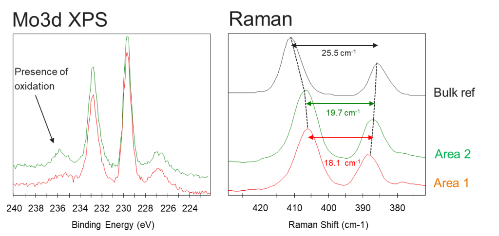
While SEM can easily visualise 2D materials, these layers are typically too thin to be easily characterised with EDX analysis. XPS, meanwhile, cannot easily resolve surface structures, but can clearly detect what material is present and quantify any chemical changes that might occur to it. It may also be helpful to bring in a Raman spectrometer alongside XPS analysis to provide a clearer idea of the number of layers in the 2D material.
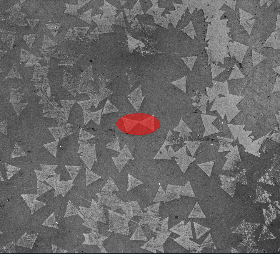
In this case study, SEM can provide high-resolution imaging to visualise the distribution of MoS₂ layers on a silicon oxide substrate. XPS can offer quantitative chemical composition data, revealing areas with varying concentrations of molybdenum and identifying the presence of both MoS2 and its oxidised form, MoO3.
In addition, a Raman spectrometer alongside XPS analysis can provide complementary information about the chemistry of the materials as well as some of its 2D material properties such as the number of layers. In this case, the number of layers in MoS2 can be identified to distinguish between single-layer and multi-layer regions.
Correlative Imaging and Surface Analysis (CISA) workflow can be of great importance for 2D materials. Moreover, the CISA Workflow is not limited to just one field of research; it has broad applications across industries that rely on detailed material analysis. Whether a materials scientist wants to improve coating performance, optimise alloy compositions or study surface degradation, the workflow enables a more comprehensive approach to understanding material behaviour without the complexity of handling data from multiple sources.
You can learn more about the CISA Workflow from Thermo Fisher and download a CISA e-book by visiting the website. Thermo Fisher Scientific is organising an XPS workshop at the East Grinstead office on 5 November 2025 that will explore state-of-the-art surface analysis capabilities such as XPS, UPS, ISS and REELS. If interested, please send a message to yahya.zakaria@thermofisher.com to receive updated information.
Manufacturing & Engineering Magazine | The Home of Manufacturing Industry News